Dholera, Gujarat:
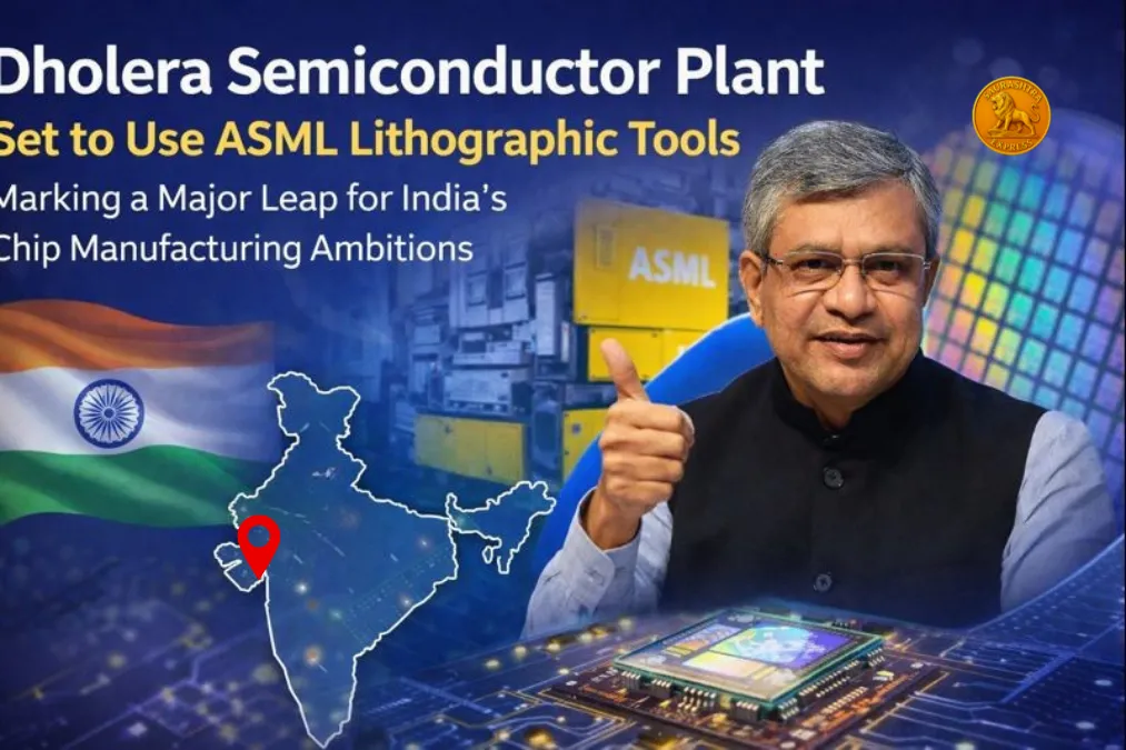
India’s long-term push to build a globally competitive semiconductor ecosystem has entered a decisive new phase, with confirmation that the Dholera Semiconductor Plant will deploy advanced lithographic tools supplied by Dutch technology giant ASML. The announcement was made by Union Minister for Electronics and Information Technology Ashwini Vaishnaw during his official visit to the Netherlands, where he toured ASML’s headquarters in Veldhoven to gain firsthand insight into the company’s cutting-edge chipmaking technologies.
The decision to incorporate ASML’s highly specialised lithography equipment places the Dholera Semiconductor Plant among a select group of advanced fabrication facilities worldwide that rely on the Dutch firm’s tools for precision chip production. It also signals India’s serious intent to move beyond chip design and into high-value manufacturing, a segment long dominated by East Asian and Western economies.
Minister’s Visit Underscores Strategic Importance
During his visit to ASML’s facilities, Minister Vaishnaw highlighted the strategic importance of the partnership, noting that lithography lies at the heart of semiconductor manufacturing. Speaking on the sidelines of the visit, he said that the Dholera fab would use ASML equipment, underlining why it was essential for Indian policymakers to understand the technology directly from its source.
Lithography, the process of printing intricate circuit patterns onto silicon wafers, is among the most complex and capital-intensive stages of chip production. Mastery of this process determines not only the performance of semiconductors but also their efficiency, reliability, and scalability. ASML, widely regarded as the global leader in lithographic systems, is currently the only company capable of producing the most advanced tools used in cutting-edge chip manufacturing.
An official statement confirmed the minister’s presence at ASML’s Veldhoven site, describing the visit as part of India’s broader engagement with global technology leaders to strengthen domestic semiconductor capabilities.
Tata Group Leads India’s Flagship Fab Project
At the centre of this ambitious effort is the Tata Group, which is spearheading the Dholera Semiconductor Plant project. The proposed fabrication facility represents one of the largest industrial investments in India’s recent history, with a projected outlay of approximately ₹91,000 crore.
The scale of public support for the project underlines its national importance. The central government has committed to providing 50 per cent fiscal support on a pari-passu basis, while the Gujarat state government will contribute an additional 20 per cent. This collaborative funding model reflects a shared commitment between the Centre and the state to establish India as a credible semiconductor manufacturing destination.
For Tata Group, the project marks a strategic expansion into advanced electronics manufacturing, complementing its existing footprint in technology services, electronics assembly, and global supply chains. For India, it represents a foundational step toward reducing dependence on imported chips, which are critical components in everything from smartphones and automobiles to defence systems and renewable energy infrastructure.
Why ASML Matters to the Dholera Semiconductor Plant
ASML’s role in global semiconductor manufacturing is difficult to overstate. The company supplies lithography systems that are indispensable for producing modern chips, particularly those used in high-performance computing, artificial intelligence, telecommunications, and consumer electronics.
Lithographic tools work by projecting patterns onto silicon wafers using highly precise light sources, enabling the creation of billions of transistors on a single chip. As chip sizes shrink and performance demands increase, the technology required becomes exponentially more complex. ASML has spent decades refining this capability, making its equipment a cornerstone of advanced semiconductor fabs worldwide.
By confirming that the Dholera Semiconductor Plant will use ASML lithographic tools, India has signalled that it intends to compete not just at the lower end of chip manufacturing but also in more sophisticated segments of the market. This move aligns with the government’s stated goal of creating an end-to-end semiconductor ecosystem that spans design, fabrication, testing, and packaging.
A Turning Point for India’s Semiconductor Journey
India’s semiconductor story has historically been defined by strong design capabilities but limited manufacturing capacity. Indian engineers play a significant role in chip design for global companies, yet the physical fabrication of chips has largely taken place overseas.
That imbalance has become increasingly problematic in recent years, as global supply chain disruptions exposed the risks of over-reliance on a small number of manufacturing hubs. Recognising this vulnerability, India launched a comprehensive semiconductor mission aimed at attracting investment, building infrastructure, and fostering partnerships with global technology leaders.
The Dholera Semiconductor Plant is widely viewed as the flagship project of this mission. Its adoption of ASML technology represents a critical validation of India’s readiness to host advanced manufacturing processes that meet global standards of quality and precision.
Growing Interest from Global Equipment Makers
Minister Vaishnaw noted that ASML’s engagement with India is part of a broader trend, with several global equipment manufacturers now exploring opportunities to establish or expand their presence in the country. This growing interest is driven by a combination of factors, including India’s expanding electronics market, its large pool of skilled engineering talent, and the policy stability offered by the current government.
Prime Minister Narendra Modi’s consistent emphasis on manufacturing, technology self-reliance, and ease of doing business has helped create an environment that global firms increasingly view as attractive. Incentive schemes, streamlined regulations, and long-term policy clarity have further strengthened India’s pitch as a viable alternative to traditional manufacturing hubs.
ASML itself announced plans last year to expand its operations in India, a move widely interpreted as a sign of confidence in the country’s semiconductor ambitions. While ASML’s core manufacturing remains in Europe, its growing engagement with India reflects the strategic importance of the market in the company’s long-term outlook.
Gujarat’s Role as a Semiconductor Hub
The choice of Dholera, located in Gujarat, as the site for India’s flagship semiconductor fab is no coincidence. The region has been developed as a Special Investment Region, offering large tracts of land, modern infrastructure, and proximity to ports and logistics networks.
Gujarat’s proactive industrial policies and track record of hosting large-scale manufacturing projects have made it a preferred destination for investors. The state government’s decision to contribute 20 per cent of the project’s fiscal support further underscores its commitment to positioning Gujarat as a major hub for high-technology manufacturing.
Once operational, the Dholera Semiconductor Plant is expected to generate thousands of direct and indirect jobs, stimulate ancillary industries, and catalyse the development of a broader electronics manufacturing ecosystem in the region.
Implications for India’s Economy and Technology Sector
The establishment of a semiconductor fab equipped with ASML lithographic tools has far-reaching implications for India’s economy. Semiconductors are foundational to modern technology, and domestic manufacturing capability can significantly enhance economic resilience.
For industries such as automotive manufacturing, renewable energy, telecommunications, and defence, access to locally produced chips can reduce costs, improve supply chain security, and accelerate innovation. For startups and research institutions, the presence of advanced fabrication facilities can open new avenues for experimentation and product development.
From a geopolitical perspective, the Dholera Semiconductor Plant strengthens India’s position in the global technology landscape. As countries around the world seek to secure their semiconductor supply chains, India’s emergence as a credible manufacturing location enhances its strategic relevance and bargaining power.
Challenges Ahead Despite Optimism
While the announcement marks a major milestone, industry experts caution that building and operating a semiconductor fab is an extraordinarily complex undertaking. Beyond the installation of advanced equipment, success depends on factors such as process expertise, supply chain integration, skilled manpower, and sustained policy support.
Lithographic tools from ASML are among the most sophisticated machines ever built, requiring precise environmental controls, specialised maintenance, and highly trained operators. Ensuring that the Dholera Semiconductor Plant can consistently meet these requirements will be critical to its long-term viability.
Nevertheless, the strong backing from both the central and state governments, combined with Tata Group’s industrial experience and ASML’s technological leadership, provides a solid foundation for addressing these challenges.
A Signal to the World
The collaboration between Tata Group and ASML sends a clear message to the global semiconductor industry: India is ready to play a more significant role in chip manufacturing. By investing in advanced lithography and committing substantial public resources, the country is positioning itself as a serious contender in a field that underpins the modern digital economy.
As more international players assess India’s progress, the Dholera Semiconductor Plant could become a reference point for future investments, attracting additional technology partners, suppliers, and research collaborations.
Also read: Dholera Emerges as the Epicenter of Gujarat’s Economic Transformation
Conclusion:
As India continues to roll out its semiconductor strategy, the focus will increasingly shift from announcements to execution. The successful deployment of ASML lithographic tools at the Dholera Semiconductor Plant will be closely watched by industry observers, policymakers, and global markets alike.
If implemented as planned, the project has the potential to reshape India’s technology landscape, reduce strategic vulnerabilities, and unlock new economic opportunities. More importantly, it represents a tangible step toward realising India’s ambition of becoming a global hub for advanced manufacturing and innovation.
With strong government backing, a trusted industrial partner in Tata Group, and world-class technology from ASML, the Dholera Semiconductor Plant stands as a symbol of India’s determination to secure its place in the future of global semiconductor production.